PCB Design and Assembly
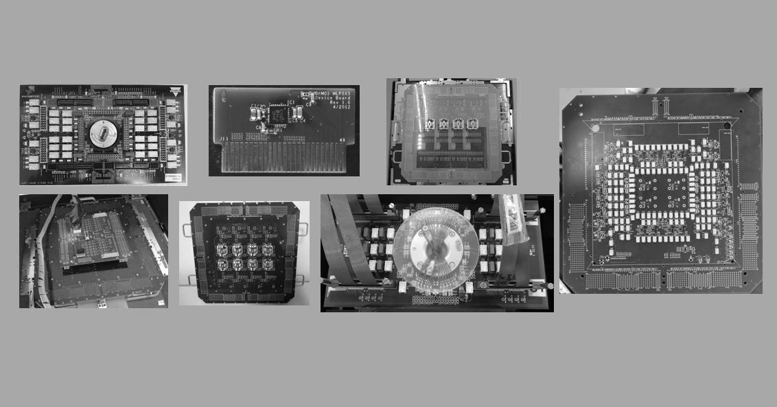
Our Test PCBs
We specialize in creating custom test applications (hardware and software) for both Eagle Test and J750 platforms. With over 25 years of combined experience, our team brings extensive expertise in schematic and PCB design, coding, and debugging to provide end-to-end customer qualification support.
- Review Customer Test Specification
- Test Schematic Design
- BOM
- Layout and Assembly
- Coding
- HW and SW Debugging
- Correlation and GR&R
- Device Characteization at Temp.(as needed)
- Installation
- Qualification Lot Run
Our Capabilities from Previous Projects
We offer end-to-end hardware development, from schematic entry, layout, gerber, to assembly.
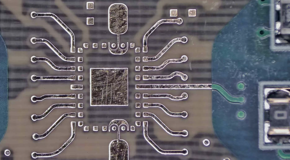
PCB Design Capabilities
| PCB Design Software | Cadence Allegro, Mentor Graphics |
|---|---|
| PCB Design for Test Engineering, etc. | ATE Board, Load Board, DUT Board, Probe Card, Pass-Through Board, Bridge Board, Universal Board, Diagnostic Board, Interposer Board |
| Special PCB Design Specs | High Voltage - 1250V, Low Leakage - 100pA, High Current - 100A, High Speed - 50Mhz |
| Min. line width/space | 3/3mil |
| Min. Drilling Size (Mechanical) | 0.15 mm (5.9mils) |
| Buried / Blind Via | 0.1mm (3.93mils) |
| Max. Finishing Board Size | 416mm x 416mm |
| Min. Board Thickness | 1.57mm (62mils) |
| Max. Board Thickness | 4.76mm (187.4mils) |
| Aspect ratio | 21:1 |
| Material | FR4 TU-768/IT-180A, R-5775G |